Design Question - Clock Dividers and Duty Cycle
The ubiquitous Divide-by-3 Counter with 50% Duty Cycle and its siblings.
In RTL Design interviews, it's common to encounter questions about clock divider circuits. While many interviewees might have quick answers ready from a cursory Google search, this topic has much more depth that often goes unexplored. This post aims to delve into practical implementations, going beyond general knowledge.
Need for a Clock Divider
Clock divider circuits reduce clock frequency for slower components, generate multiple clocks, and synchronize data between different clock speeds. They manage power by enabling slower speeds, adjust timing, and are used in PWM and motor control. They aid in serial communication, simplify testing by slowing speeds, and are crucial in digital filters for specific sampling rates.
Interview Questions
- Design a Clock Divider circuit to divide the input clock by a factor of 4 (or any other power of 2)
- Design a Clock Divider circuit to divide the input clock by a factor of 3 (or any other odd number)
- Modify the design to generate an output clock with 50% duty cycle
Solution - Divide by 4 Circuit
The divide by 4 (or any other power of 2, or for that matter any even number) circuit is a simple counter that runs from 0 to n-1 (in this case, 3) and then rolls over back to 0.
If you are dividing the incoming clock by a factor of 4, the output should have one rising edge for every set of four rising edges of the input clock.
The counter cycles through the values 0, 1, 2, 3. For two consecutive states of the counter, the output should be a 0, and for the other two states it should be a 1.
A snippet of code for the Divide by 4 counter -
logic [ 1: 0]  sig_div4_cnt;

// Divide by 4 counter
always_ff @(posedge clk)
begin
   if (rst)
   begin
      sig_div4_cnt <= '0;
   end
   else
   begin
      sig_div4_cnt <= sig_div4_cnt + 1;
   end
end

// Generating the divided down version of clk
assign clk_div_4 = sig_div4_cnt[1];
Divide by 4 Counter
In the above example, the MSB of the 2-bit counter is used to hold the output LOW in counter states 0 and 1, and HIGH in the other two states of the counter.
One additional advantage of implementing the output this way, instead of using a case or an if-else statement is that the output is sequential, as opposed to combinatorial.
Can you figure out a way to generate the output clock with a 25% duty cycle?
Solution - Divide by 3 Circuit
Division by odd numbers is where things start getting a little trickier. The design concept is still the same as the earlier example. We have a 2-bit counter that runs from 0 to 2 and then gets reset to 0. The counter now has 3 states, 0, 1 and 2. Assuming we do not have the 50% duty cycle requirement, we can simply design the circuit as follows -
logic [ 1: 0]  sig_div3_cnt;

// Divide by 3 counter
// No duty-cycle management
always_ff @(posedge clk)
begin
   if (rst)
   begin
      sig_div3_cnt <= '0;
   end
   else if (sig_div3_cnt == 2'd2)       // Roll over back to 0
   begin
      sig_div3_cnt <= '0;
   end
   else
   begin
      sig_div3_cnt <= sig_div3_cnt + 1;
   end
end

// Generating the divided down version of clk
assign sig_clk_div_3 = (sig_div3_cnt == 2) ? 1'b1 : 1'b0;
assign clk_div_3     = sig_clk_div_3;
Divide by 3 Counter
This generates an output clock with 33% duty cycle.

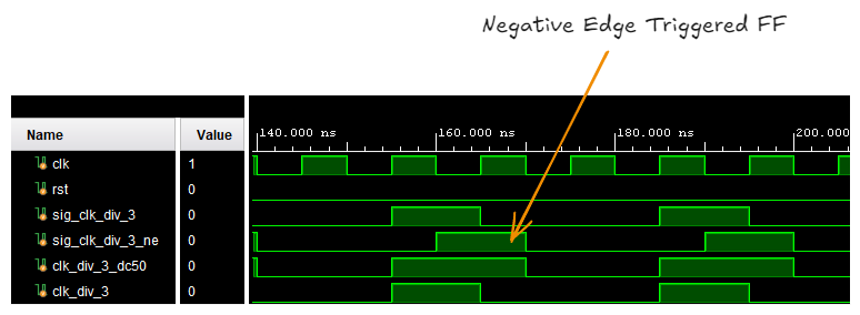
In order to create an output with 50% duty cycle, we need the output, clk_div_3 to be asserted for another half clock cycle. Referring to the diagram below, the extended output is shown in orange.

In order to drive any signal for half a clock cycle, we have to utilize the negative edge of the clock.
Let's take the Divide by 3 circuit explained earlier and add this additional functionality.
// For 50% dutycycle, we need the output to be asserted
// for half a clock cycle more
always_ff @(negedge clk)
begin
   sig_clk_div_3_ne <= sig_clk_div_3;
end

// Generating the divided down version of clk (50% duty cycle)
assign clk_div_3_dc50 = sig_clk_div_3 | sig_clk_div_3_ne;
Divide by 3 Counter (with 50% duty cycle)

The primary downside of this design is that the generated output signal is combinatorial.
Practical Considerations for FPGA Design
This is an absolutely horrible way to generate divided down versions of the master clock in an FPGA design. Clocks in an FPGA have a certain status and have their own exclusive, low-jitter distribution routing. Signals from the FPGA fabric cannot easily enter this special clock routing network. As can be seen from above examples, the generated clocks are either on the Q output of a Flip-Flop or are purely combinatorial. Driving a bunch of sequential logic from a clock generated in this manner will cause a lot of issues in an FPGA.
For the 50% duty cycle design, one must realize that the path from sig_clk_div_3 to sig_clk_div_3_ne is required to be traversed in half a clock cycle. This puts an extra burden on the synthesis tools.
Considerations for Clock Dividers in an FPGA
Xilinx FPGAs have dedicated clock management resources that can take care of clock division. Users have access to PLLs and their superset, MMCMs (Mixed Mode Clock Managers). For simple division, the Xilinx primitive BUFGCE_DIV can be used.
Takeaways
While these questions are understandable for interview purposes, it is important to recognize that, in proactive, clock division in FPGAs is typically achieved using dedicated FPGA primitives. Achieving a 50% duty cycle output clock becomes complex when dealing with odd division factors and requires utilizing both clock edges.