The Fundamentals of Static Timing Analysis in Digital Circuits
Setup and Hold Time, Critical Paths and Other Key Concepts Explained
Static Timing Analysis (STA) is a method of validating the timing performance of a digital circuit by checking all possible paths for timing violations. STA breaks a design down into timing paths, calculates the signal propagation delay along each path, and checks for violations of timing constraints inside the design and at the input/output interface.
⏱️Static Timing Analysis is a broad field, and the intricate language used in the literature can obscure some of the fundamental ideas. This is an attempt to clarify the concepts and give a conceptual rundown of the procedure.
Types of STA Paths
As shown in the figure below, a design will have different types of timing paths.
The cloud of logic shown in the diagram might contain multiple combinatorial paths. The STA tool uses the shortest path to compute the minimum delay and the longest path to compute the maximum delay. We will look at these concepts later to understand why both these computations are important.
Let's look at all the paths shown here in detail -
- Path #1: This is a path from an input port to the data input of a sequential element.
- Path #2: This is the path from the clock pin of a sequential element to the data pin of the next sequential element, traversing through a cloud of combinatorial logic. We generally focus on this path during the timing closure process.
- Path #3: This path goes from the clock pin of a sequential element to an output port.
- Path #4: This is a purely combinatorial path from the input to the output port.
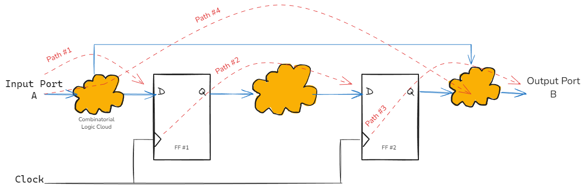
In addition to the 4 paths described above, there are a few more path types that need to be accounted for during STA. These are as follows -
- Clock Path: The clock distribution network from the clock source to the clock pin of sequential elements. This path consists of one or more clock buffers (and optionally, inverters). Clock path delays (also known as clock skew) can result in tightening or loosing the data path timing constraints.
- Asynchronous Path: This is a path from an input pin to an asynchronous set or reset pin of a sequential element. This is required for recovery and removal checks.
Timing Path between Sequential Elements (Path #2)
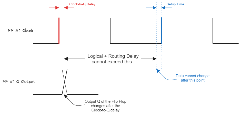
It is important to understand all the elements in this path conceptually, and then build upon that knowledge for further discussion. This path can be further broken down into the following elements (for setup checks) -
- Clock-to-Q Delay: This is the time required for the flip-flop input data (D) to show up at the output (Q) after the active clock edge.
- Propagation Delay: This is the time required for the data to propagate through the combinatorial logic cloud. The propagation delay can be further broken down into -
- Logical Delay - This is the delay through the logical elements in the path.
- Routing Delay - This is the delay through the connecting wires.
- Setup Time of the Destination Flip-Flop: This is the time period before the clock edge, when the data should be stable to be captured correctly by the destination flip-flop.
A rule of thumb is that the routing delay should generally not consume more than 60% of the clock period.
In addition to the setup checks, there are hold time checks as well.
Hold Time is the time period after the clock edge, when the input data must be stable, so that it is correctly latched by the flip-flop.
Critical Path and Slack
Critical Path in a design is the longest combinatorial path between two sequential elements (such as flip-flops or registers). The maximum time required for the data to propagate from one sequential element to the next is determined by the length of the critical path. This has a direct bearing on the maximum clock frequency that the digital logic can run at.
MaximumClockFrequency=1/TimeRequiredtoTraversetheCriticalPath
In a real world scenario, we are trying to design modules to meet timing closure at a given target clock frequency. The total time for a signal to travel from the source flip-flop to the destination flip-flop can be given (loosely[1]) by the following equation.
Ttotal=Tclk−to−q+Tlogic+Trouting+Tsetup
Clock-to-Q and setup time of flip-flops are generally known beforehand. Designers have to manage the routing and logical delays, so that the total delay is less than the required clock period.
Slack is the difference between the required time period and the actual arrival time of the signal at a particular point in the circuit. When the signal arrives earlier than the required time, the slack is said to be positive. This indicates that all setup time requirements are met (along with some extra margin). Negative slack is when the signal arrives later than the required time, thereby violating the setup time of the destination flip-flop.
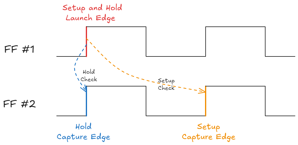
Setup and Hold Checks
A setup check determines whether all setup time constraints are met, while a hold check determines the same for hold time constraints. It is important to introduce the concept of a launch edge and a capture edge.
Launch Edge is the edge of the clock on which the source flip-flop launches the data.
Capture Edge is the edge of the clock on which the destination flip-flop captures the data.
Since, the data travels from the source to the destination, and has to reach there before the setup time window begins, setup checks are performed at the Capture Edge.
Hold check ensures that the hold time requirements at the source flip-flop are met, i.e. the data does not change during the duration of the Hold window. Hence, hold checks are performed at the Launch Edge.
🚨 A caveat to the above paragraph is the Hold Checks are made one clock edge prior to the Capture Edge (by the STA tools). This checks out with our example because the Launch Edge is always one clock cycle prior to the Capture Edge.
💡Potential problems can arise when multi-cycle paths are used in the design.
Minimum and Maximum Delays through Combinatorial Logic
Maximum delays through combinatorial logic affect setup checks, because the signal might be delayed reaching the destination. Minimum delays on the other hand, affect hold checks, because the data might transition too fast and not remain stable through the duration of the hold window.
In most modern FPGAs, sequential elements have zero or even negative hold time requirements. Unless there are some sub-optimal design elements, leading to a large clock skew, it is very hard to see hold time violations.
Coming up in the Next Edition
After laying down the foundational concepts of Static Timing Analysis, we will take a look at some more advanced concepts in the next edition. These include things like clock skew, clock jitter, timing exceptions (false paths and multi-cycle paths) and how to mitigate timing closure issues.
- For completeness, elements like, clock skew, jitter and clock uncertainty should also be considered. Adding too many elements at the same time, obfuscates the primary concepts. Therefore, some of these elements have been left out from the explanation at this point.