Rethinking Resets: Best Practices for FPGA Design
While designing an RTL module, most engineers do not even give a second thought to the reset signal. Every textbook on the subject touches upon the pros and cons of synchronous vs asynchronous resets. The texts generally focus on the correct syntax for inferring a synchronous or an asynchronous reset. It is almost drilled into our brains that every sequential element in the design needs to have a reset (and this is almost always true in the ASIC world). The ubiquitous nature of reset signals do warrant that we pause for a moment before we blindly connect a reset signal to every flip-flop in the design, while working with FPGAs.
Take a Step Back and Consider This
What is the true purpose of the reset in your design? 🤔
In general terms, the purpose of a reset signal can be summarized as follows:
- Power-On Reset: To initialize all sequential elements in your design to a known state at power-up.
- Software Reset: To initialize specific sequential elements to a known good state during operation, such as resetting a locked-up state machine.
- Hardware Reset: To use an internally generated signal or an external input to reset all or some portions of your design during operation.
The Problem with Resetting Everything in the FPGA
FPGA fabrics are rich in registers. Simply connecting the reset signal to all registers in the design can place a heavy load on the Place and Route tools during the routing phase. A high fanout signal like reset can significantly impact the maximum clock frequency, area, and power consumption.
Wouldn’t the Logic Fail Functional Equivalence Without an Initialization Reset?
In Xilinx FPGAs, every Flip-flop is connected to the GSR (Global Set/Reset) line, which ensures that every Flip-flop will come up in the desired state ('0' or '1'), without the need for an explicit initialization reset.
The initial value can be specified in SystemVerilog as follows -
logic       reg1 = 1’b0;    // specifying reg1 to initialize to a zero
logic       reg2 = 1’b1;    // specifying reg2 to initialize to a one
logic [3:0] reg3 = 4’b1011; // specifying INIT value for 4-bit register
Specifying initial values for registers
💡If no initial value is provided, the synthesis tool is at a liberty to assign either a '0' or a '1' to a particular element. Vivado synthesis generally defaults to a '0', with a few exceptions such as one-hot encoded state machines.
For Software Resets and external Hardware Resets, it is necessary to code the reset logic explicitly.
Some other scenarios where the use of Resets can cause issues
Inferred synchronous code might be mapped to resources such as -
- LUTs
- Registers
- SRLs
- BlockRAM, UltraRAM or Distributed LUT memory
- DSP48s
The choice and usage of resets, along with the coding style, can significantly impact the selection of optimal resources. Here are a couple of examples: - Shift Registers: A 32-bit shift register can be efficiently mapped to a single LUT in a Xilinx UltraScale+ device. However, if the logic includes a reset signal, the synthesis tool might map the same logic into 32 discrete registers, which is less efficient.
- Multipliers: Using an asynchronous reset on a multiplier might result in the associated registers being placed in the fabric logic instead of the more efficient DSP48s.
Some Real-Life Observations and Notes
Wide Data Buses: Wide data buses with multiple pipeline stages typically do not require a reset. This can simplify the design and improve performance.
Synchronous Resets: Xilinx recommends using synchronous, active-high resets wherever possible. Active-low resets require an inverter, which can sometimes be absorbed into the register but may also necessitate a LUT, adding an extra logic level to the path.
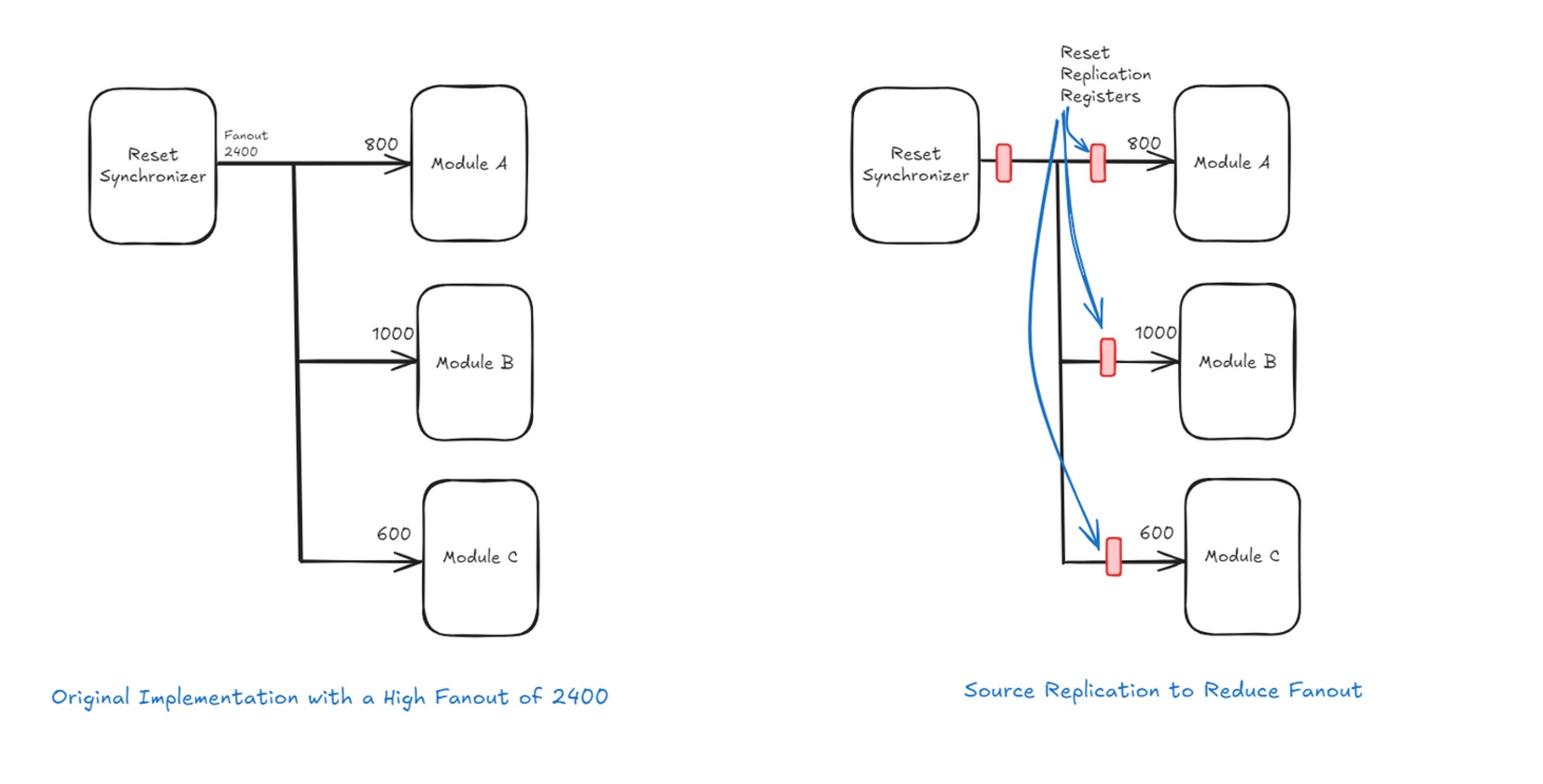
High Fanout Reset Issues: High fanout reset signals can be problematic. To mitigate this, you can replicate the source of the reset signal to balance the load on the reset net.
Global Clock Buffer (BUFG): In extreme high-fanout scenarios, a global clock buffer (BUFG) can be used to route the reset signal. However, this approach is generally not recommended due to potential timing issues.
SSI Devices: In SSI (Stacked Silicon Interconnect) devices, timing closure on reset paths behaves similarly to other paths. Designers should account for additional pipeline stages when crossing SLR (Super Logic Region) boundaries to ensure proper timing closure.