Beyond Basic Gates: How Multiplexers Map to LUTs and the Power of Xilinx F7, F8 MUXes
Understanding Xilinx UltraScale CLB architecture is necessary to fully harness the power of expansion multiplexers which can be cascaded at the output of LUTs.
In the intricate world of FPGA design, some components are so fundamental they become almost invisible. The multiplexer (MUX) is one such unsung hero. From selecting data paths in a processor to directing signals in a complex communication protocol, MUXes are everywhere. But have you ever stopped to consider how these critical data selectors are actually implemented within the vast, reconfigurable fabric of a Xilinx FPGA?
This article will pull back the curtain, demystifying how MUXes map from your HDL code onto the underlying hardware. We'll start with how simple MUXes fit neatly into Look-Up Tables (LUTs), then explore the challenges of building wider MUXes, and finally, reveal the elegance and power of Xilinx's dedicated F7 MUX for high-performance 8:1 multiplexing.
I. The Basics: Mapping Small MUXes to LUTs
At its core, a multiplexer is a data selector. It takes multiple input data lines, a set of select lines, and outputs just one of the input data lines based on the binary value of the select lines. If a MUX has 'N' data inputs, it requires 'M' select lines where 2M=N.
In Xilinx 7-series and UltraScale FPGAs, the primary combinational logic element is the 6-input Look-Up Table (LUT6). A LUT6 can implement any Boolean function of its 6 inputs.
💡Implementing a 2:1 MUX in a LUT
Let's start with the simplest case: a 2:1 MUX. This MUX has two data inputs (e.g., I0, I1) and one select line (S0). It effectively chooses between I0 or I1.
A 2:1 MUX requires only 3 inputs in total (I0, I1, S0). This fits comfortably within a LUT6. The synthesis tool will configure a LUT6 to implement this function. This consumes just one level of LUT logic.
💡Implementing a 4:1 MUX in a LUT
Now consider a 4:1 MUX. This requires four data inputs (e.g., I0 through I3) and two select lines (S0, S1). The total number of inputs for this function is 4+2=6.
A 4:1 MUX maps perfectly to a single LUT6, utilizing all its inputs. This still consumes one level of LUT logic. This demonstrates the efficiency of the LUT: any combinational function with up to 6 inputs can be implemented in a single LUT, meaning minimal propagation delay (one logic level).
III. The Challenge: Building Wider MUXes with Only LUTs
The efficiency of mapping small MUXes to single LUTs runs into a hard limit: the fixed number of inputs on a LUT (typically 6 for Xilinx).
Consider the requirements for an 8:1 MUX:
- 8 data inputs
- 3 select lines (since 23=8)
- Total inputs required = 8+3=11 inputs.
Clearly, an 8:1 MUX cannot be implemented by a single LUT6. If only general-purpose LUTs were available, the synthesis tool would have to break it down and rely on LUT chaining:
- You'd typically use two 4:1 MUXes (each implemented by one LUT) to handle the first four inputs and the next four inputs, respectively, based on the lower two select lines.
- The outputs of these two 4:1 MUXes would then feed into a third 2:1 MUX (implemented by another LUT), which is controlled by the most significant select line.
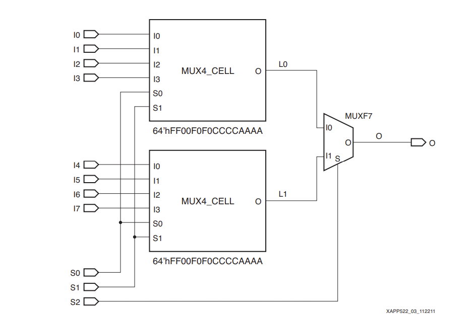
In this purely LUT-based approach, the 8:1 MUX consumes 3 LUTs. More importantly, the critical data path (from a data input through the MUXes to the output) would traverse two distinct levels of LUT logic (e.g., Data Input -> 4:1 LUT -> 2:1 LUT -> Output). This cascading introduces increased propagation delay, directly impacting the maximum clock frequency your design can achieve. For even wider MUXes (e.g., 16:1 or 32:1) built solely with LUTs, the number of cascaded LUT levels would grow further, leading to severe performance bottlenecks.
IV. Xilinx's Solution: The Dedicated F7 MUX
To overcome the performance limitations of LUT-only MUX chaining, Xilinx FPGAs incorporate specialized, dedicated hardware blocks for wide multiplexing.
The key dedicated element for 8:1 multiplexing is the F7 MUX. The F7 MUX is not a general-purpose LUT; it's a pre-optimized, hardwired logic block specifically engineered to implement an 8:1 multiplexer with remarkable efficiency.
Crucially, the F7 MUX significantly optimizes the path for an 8:1 MUX. While the overall 8:1 MUX structure still involves an initial stage of LUTs (to handle the 4:1 selections), the F7 MUX acts as a highly optimized, extremely fast single dedicated stage to combine these results. This effectively collapses what would have been a slower, full LUT-based final stage into a much faster, dedicated MUX element. This dedicated path ensures minimal propagation delay for the 8:1 selection, leading to far superior overall performance compared to a purely LUT-chained approach.
V. Advantages of Using Dedicated F7 MUXes
The inclusion and automatic inference of dedicated F7 MUXes offer profound advantages for FPGA designers:
- Superior Performance: This is the most significant benefit. By utilizing a highly optimized, dedicated MUXF7 for the critical selection stage, propagation delays are dramatically shortened. This enables much higher achievable clock frequencies for designs involving wide data selection compared to an all-LUT implementation.
- Resource Efficiency: Utilizing dedicated hardware elements means less reliance on general-purpose LUTs, which are freed up for other complex combinational logic functions. This contributes to more efficient overall resource utilization.
- Predictable Timing: Dedicated MUX elements have optimized and well-characterized delays, making their timing behavior more consistent and predictable. This simplifies timing closure and debugging in high-performance designs.
VI. Inferring F7 MUXes in SystemVerilog
For designers, the good news is that you typically don't need to explicitly instantiate F7 MUX primitives. Modern synthesis tools, such as Vivado for Xilinx devices, are highly intelligent. When they encounter a standard HDL construct that represents an 8:1 multiplexer, they will automatically recognize the pattern and infer the dedicated F7 MUX.
AMD Xilinx's documentation, specifically recommends using case statements for clear and efficient MUX inference:
module eight_to_one_mux (
    input [7:0] data_in,     // 8 data inputs
    input [2:0] sel,         // 3 select lines for 8 inputs
    output reg data_out
);

always_comb begin
    case (sel)
        3'b000: data_out = data_in[0];
        3'b001: data_out = data_in[1];
        3'b010: data_out = data_in[2];
        3'b011: data_out = data_in[3];
        3'b100: data_out = data_in[4];
        3'b101: data_out = data_in[5];
        3'b110: data_out = data_in[6];
        3'b111: data_out = data_in[7];
        default: data_out = '0;
    endcase
end

endmodule
It's also worth noting that Xilinx devices offer even wider dedicated MUX blocks like F8 MUXes (for 16:1 multiplexing). These are built by cascading lower-level dedicated MUX elements, always striving to minimize combinational depth and maximize performance.
VII. Conclusion
Understanding how multiplexers map to FPGA hardware is a vital piece of architectural knowledge for any serious FPGA designer. While simple MUXes map efficiently to single LUTs, the demands of wider data selection quickly expose the limitations of LUT chaining. Xilinx's dedicated F7 MUX blocks (and their wider counterparts like the F8) provide an elegant and highly optimized solution, allowing for the construction of high-performance MUX trees.
✒️References
- Xilinx Application Note - Multiplexer Design Techniques for Datapath Performance with Minimized Routing Resources Application Note (XAPP522)
- Xilinx User Guide - UltraScale Architecture Libraries Guide (UG974)