Advanced Topics in Static Timing Analysis
Understanding Clock Skew, Clock Jitter and effects of additional pipelining on latency.
Before moving on to some of the more in-depth topics about Static Timing Analysis (STA) and Timing Closure, it is important to introduce and intuitively understand two terms related to clock distribution -
- Clock Skew, and
- Clock Jitter
Clock Skew
Clock skew refers to the difference in the clock arrival time at different sequential elements in the design. Although extreme care is taken to route the clocks over load balanced and length matched low-skew routing, it is impossible to completely eliminate clock skew in any digital circuit.
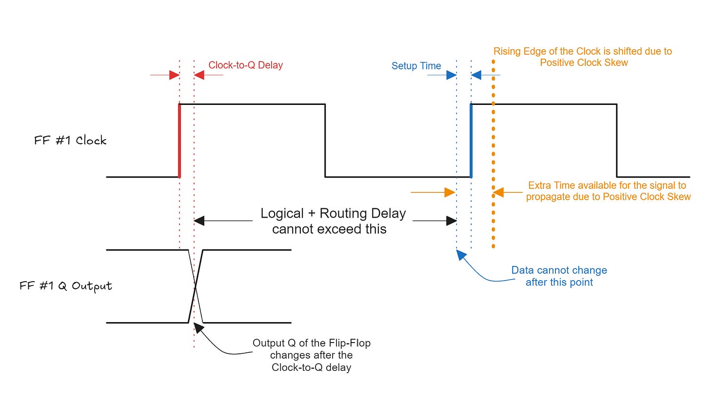
The presence of clock skew impacts STA and affects timing closure (but at times can work in our favor as well).
Positive Clock Skew is present when the clock reaches the destination flip-flop later than the source flip-flop. This situation helps the setup checks by increasing the amount of time available for the data signal to travel from the source to the destination flip-flop. At the same time, a positive skew conversely affects the hold time constraints, since there is a chance that the data might change too soon with respect to the destination clock edge.
Negative Clock Skew works in exactly the opposite way. Intuitively, it can be seen that the data will have a smaller time window to reach the destination flip-flop if the destination edge moves to the left (as compared to it's ideal location). Negative clock skew is worse for setup paths but help with hold checks.
Clock Jitter
Clock jitter refers to the variations and deviations in the timing of a clock signal's edges from their ideal positions. In other words, these are small, unpredictable changes in the timing of a clock pulse.
As a Digital, RTL designer, one does not too much control on the jitter aspects of the clock. These are generally managed during the board design phase of the project, by choosing the appropriate clock sources, power supplies and reducing EMI (Electromagnetic Interference). At the FPGA design level, using clock conditioning blocks like PLLs or MMCMs, will help clean the clock signal and reduce jitter.
Jitter adds uncertainty and the STA tools will have to reduce the available timing window to account for this unpredictability.
Interview Question
One of the most commonly asked interview questions is -
What can you do to achieve timing closure or increase the working clock frequency of your design?
99% of the candidates that I have interviewed, always lead with Pipelining as the first thing they would do.
In theory, this is not an incorrect answer, but there are a few pre-requisites to adding pipelines in the design. The first step is to figure out the cause of the timing failure. If you have a long route, by all means, add enough pipelines to break the critical path. But, what if the timing closure issues are because of high-fanout nets, or even worse, localized congestion in the FPGA. Adding pipelines would actually be detrimental to the final goal of achieving timing closure.
A follow up question is about design trade-offs. You gain something, you lose something. What's the thing that you lose when you add pipelines?
- Resource usage increases with more pipeline stages. This is especially true for wide data buses.
- Adding pipelines increases the overall latency in terms of clock cycles.
💡Remember - Just because the latency increases in terms of number of clocks, does not mean that the latency has increased in terms of absolute time.
Let's take a look at an example -
Say you have a path running at 100 MHz. A signal takes one clock cycle to traverse a timing path i.e. it takes 10 ns. Now assume that you are running the same path at 200 MHz. You add a pipeline stage, so that you can meet timing at 200 MHz. Every clock cycle is now 5 ns wide. Even if you take 2 clock cycles to get from the same source to the destination, the absolute time it takes is the same (10 ns) in both cases.
Takeaways
Managing clock skew and jitter is essential to avoid timing violations. Implementing pipelining can significantly boost throughput by breaking down operations into sequential stages, despite introducing additional latency. Balancing these factors is key to optimizing the overall efficiency and robustness of digital designs.